NOTICE:
Please note that this design is not a student project, and no file(s) will be release on freebies
Phone/ Whatsapp/ Imo/ Telegram : +2348123206299
Email: acecct.18f4550@gmail.com
copyright @ T9 LEGENDARY RELIABILITY DESIGNS.
File A: (220 usd)
circuit diagram, proteus file, hex file with your company name , inductor calculation, capacitor calculation, mosfet calculation and setup video.
File B: (550 usd)
circuit diagram, proteus file, source code with compiler (Code written in Clang.), inductor calculation, capacitor calculation, mosfet calculation and setup video.
Specification:
1.Based on MPPT algorithm
2. LED indication for the state of charge
3. 16x2 character LCD display for displaying voltages,current,power etc
4. Overvoltage / Lightning protection
5. Short Circuit and Over load protection
6.Serial port data monitor
7.Synchronous operation with high and low side MOSFETS for better buck converter efficiency
8.Dual high side MOSFETS arranged back to back to prevent current leakage in low light
TECHNICAL SPECIFICATIONS:
Battery voltage: 12vdc/24vdc/48vdc
Solar max. input voltage: 100vdc
Max. current : 60A
MPPT SOLAR CHARGE CONTROLLER
Well, The most advance solar charge controller available in the market is Maximum Power Point Tracking (MPPT).The MPPT controller is more sophisticated and more expensive.It has several advantages over the earlier charge controller.It is 30 to 40 % more efficient at low temperature.But making a MPPT charge controller is little bit complex in compare to PWM charge controller.It require some basic knowledge of power electronics.
What Is MPPT ?
The Maximum Power Point Tracker (MPPT) circuit is based around a synchronous buck converter circuit..It steps the higher solar panel voltage down to the charging voltage of the battery. The Arduino tries to maximize the watts input from the solar panel by controlling the duty cycle to keep the solar panel operating at its Maximum Power Point.
The Maximum Power Point Tracker (MPPT) controller increase charge current by operating the PV module in a manner that allows the module to produce all the power it is capable of a conventional charge controller simply connects the module to the battery when the battery is discharged. When the 75W module in this example is connected directly to a battery charging at 12 volts its power production is artificially limited to about 53 watts. This wastes a whopping 22 watts or nearly 30% of the available power!
Patented MPPT technology used in this MPPT controller design operates in a very different fashion. The MPPT controller continually calculates the modules maximum power voltage, in this case 17 volts. It then operates the module at its maximum power voltage to extract maximum power. The higher power extracted from the module is then provided to the battery in the form of increased charge current. In conditions where extra PV power is not available, Sigma MPPT controller will operate as a conventional controller with very low voltage drop.

The mosfet driver
A Mosfet driver allows a low current digital output signal from a Microcontroller to drive the gate of a Mosfet. A 5 volt digital signal can switch a high voltage mosfet using the driver.A MOSFET has a gate capacitance that you need to charge so that the MOSFET can turn on and discharge it to switch off,the more current you can provide to the gate the faster you switching on/off the mosfet, that is why you use a driver.
For this design I am using a IR2104 Half Bridge driver. The IC takes the incoming PWM signal from the micro controller, and then drives two outputs for a High and a Low Side MOSFET.
Input :
First we have to provide power to the gate driver.It is give on Vcc (pin-1) and its value is in between 10-20V as per data sheet.
The high frequency PWM signal from atmega ic goes to IN (pin-2) . The shut down control signal from the atmega ic is connected on SD ( pin 3).
Output :
The 2 output PWM signals are generated from HI and LO pin. This gives the user the opportunity to fine tune the dead-band switching of the MOSFETs.
Charge Pump Circuit :
The capacitor connected between VB and VS along with the diode form the charge pump.This circuit doubles the input voltage so the high switch can be driven on. However this bootstrap circuit only works when the MOSFETs are switching.

fig1.2:
Some useful design tools
1. InductorRing program from Vladmir Denisenko (search google)

2. Power stage designer tool from Texas Instruments

3. American Wire Gauge Conductor Size Table

PCB, SIMULATION, HARDWARE AND SOLDERING:
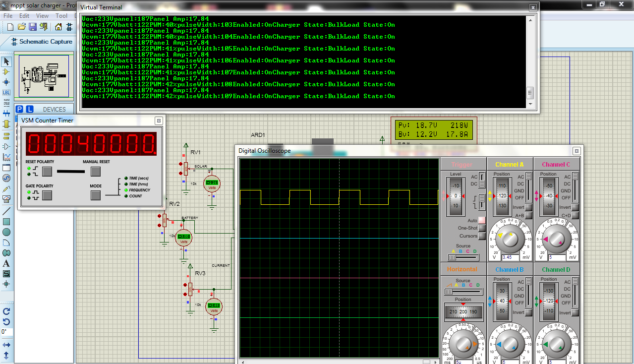
fig2.1: proteus simulation with 40khz mosfet sw..

fig2.2: printed pcb board with top sink printed

fig2.3: printed pcb board with bottom sink printed

fig2.4: Inductor design (22uH 20A)

fig2.5: printed pcb board with complete component for 12v design.

fig2.6: printed pcb board with 12vdc fan

fig2.7: testing on 150watts solar panel to charge 40ah lifepo4 battery

fig2.8: testing on 150watts solar panel to charge 40ah lifepo4 battery

fig2.9: nice packaging is needed too..
Youtube video: click here
https://www.youtube.com/watch?v=o4izARSjENg


